To start, once we take a look at the Japanese manufacturing trade as an entire—not simply meeting and semiconductors, however throughout all segments—we will observe that over the previous 25 to 30 years, Japanese producers have been going through intensifying competitors from regional rivals, particularly throughout Asia. Many of those opponents have adopted, or in some instances, immediately imitated the Japanese spirit of expertise, all whereas benefiting from considerably decrease labor prices.
This has, understandably, pushed some Japanese corporations out of the mass-market industrial house. Nevertheless, many proceed to reveal international management in extremely specialised B2B segments, resembling superior supplies, precision parts, and high-value manufacturing.
As an organization deeply concerned on this house, how would you outline the core strengths of Japanese craftsmanship and manufacturing? And the way do these examine to your regional opponents?
Thanks. Before everything, we strongly imagine that Japan’s power in manufacturing lies in our deep technological basis—particularly in areas of superior supplies, course of innovation, and engineering improvement. Japanese firms, together with ours, emphasize long-term funding in know-how and technical experience, and this has given us a aggressive edge within the international market.
In our manufacturing processes, we emphasize the shut, hands-on collaboration between expert operators and engineers. This creates a office tradition the place suggestions loops are quick, sensible challenges are solved swiftly, and processes are repeatedly improved by means of Kaizen—a uniquely Japanese philosophy of ongoing, incremental enchancment. Kaizen isn’t only a administration buzzword in Japan—it’s ingrained in our manufacturing mindset. It is what allows us to pursue high quality, effectivity, and innovation concurrently.
One other crucial power of Japanese manufacturing is the dense community of small and medium-sized enterprises (SMEs) that possess distinctive, area of interest applied sciences. These corporations are extraordinarily competent and agile, they usually play an important position in our ecosystem. For us, they’re important collaborators—whether or not we’re creating new supplies, exploring novel functions, or refining manufacturing instruments. The proximity and specialization of those suppliers permit us to conduct joint improvement rapidly and with excessive precision.
Compared to a few of our regional opponents—who could focus extra on cost-efficiency and fast scaling of facility—our method prioritizes reliability, efficiency, and long-term belief. That’s the place Japanese manufacturing continues to face out.
One of many main penalties of the COVID-19 pandemic, particularly throughout the semiconductor sector, was the worldwide chip scarcity. It triggered vital manufacturing bottlenecks throughout industries—from automotive manufacturing to electronics and computing. These disruptions revealed the vulnerability of the worldwide semiconductor provide chain and its overdependence on a restricted variety of international locations.
In response, many governments and trade leaders are actually working to regionalize manufacturing—attracting semiconductor foundries to their very own shores. Between 2021 and 2023, for instance, 18 new foundries have been established within the U.S., and related efforts are underway in Japan.
What particular alternatives does this international pattern towards regionalization and capability growth provide your organization?
The continuing regionalization of semiconductor manufacturing presents a main strategic alternative for us.
At current, our firm manufactures bonding wire and specialised supplies for semiconductor packaging and meeting. Many of the large-scale foundries and meeting corporations have historically been based mostly in East Asia, the place manufacturing has been extremely concentrated. Nevertheless, with this shift towards geographic diversification, the panorama is quickly evolving.
As international locations intention to convey semiconductor manufacturing nearer to residence, we’re seeing a redistribution of demand—and this opens new doorways for us. With extra regional foundries being established within the U.S., Europe, and different places, we now have the chance to broaden our market attain and set up new relationships in areas that beforehand sourced primarily from East Asia.
For our firm, manufacturing scale is crucial, not just for price effectivity but additionally for sustaining our technological edge. If we don’t keep a sure quantity of manufacturing, it turns into more and more troublesome to retain our edge in precision, high quality management, and R&D management we have now constructed over many years. So this growth of worldwide manufacturing is a welcome improvement—it aligns completely with our personal development aims.
In brief, quantity fuels innovation, and this international pattern empowers us to pursue each.
Because the semiconductor market expands globally, scaling operations turns into a necessity. But in Japan, this comes with distinctive challenges—most notably, demographic decline. Japan has the oldest inhabitants on the planet, and the inhabitants is shrinking annually. This impacts each the dimensions of the home market and the provision of expert labor.
How is Nippon Micrometal responding to those demographic challenges? And what position does internationalization play in your strategic planning?
This is a vital situation, and we’ve been getting ready for it strategically.
To start with, it’s necessary to know our market construction. Roughly 90% of our clients are abroad—primarily international semiconductor producers. So whereas Japan’s home market is shrinking, the international demand for semiconductors continues to develop, and our enterprise is increasing in keeping with that international pattern.
Our bonding wire is utilized in a wide selection of high-growth functions—from automotive programs and cell gadgets to AI and next-generation computing. As demand for these functions will increase globally, the necessity for high-performance bonding wire like ours will proceed to rise.
That stated, the demographic problem impacts the manufacturing workforce, particularly in Japan. To deal with this, we’re accelerating digital transformation and automation throughout our manufacturing amenities. Our objective is to scale manufacturing output whereas minimizing dependence on guide labor. We’ve invested closely in sensible manufacturing unit applied sciences and automation instruments that enhance effectivity and scale back labor pressure.
On the worldwide entrance, our philosophy is easy: manufacture as near the market as attainable. Whereas we develop core applied sciences in Japan, we’re more and more increasing our abroad manufacturing footprint. We at present have factories overseas and are actively trying to scale these operations. This method helps us handle each labor shortages and logistics prices.
Lastly, we’re additionally investing in expertise improvement right here in Japan. We rent a choose variety of high-potential engineers and help their skilled development. One in every of our key initiatives entails sponsoring engineers to pursue doctoral levels at universities. This not solely enhances our inside experience but additionally strengthens our long-term innovation capability.
In brief, internationalization is not only a method for development—it’s a necessity for sustainability.

You talked about increasing your manufacturing footprint abroad. One of many key challenges that comes with that is sustaining constant high quality throughout all manufacturing websites—particularly the excessive commonplace related to Japanese craftsmanship. How do you handle high quality management throughout your international operations?
High quality is completely paramount for us, no matter the place manufacturing happens.
In Japan, we’ve developed a extremely superior set of producing applied sciences, and we’ve created programs with centralized management that permit us to replicate that very same commonplace overseas. We now have applied a distant monitoring system that enables us to look at, management, and optimize our abroad manufacturing traces immediately from Japan. This technique captures stay manufacturing information and allows us to ship technical suggestions or corrective directions immediately.
We’ve additionally standardized our processes globally. Each abroad website receives similar tools, detailed work directions, and technical manuals. By guaranteeing uniformity in instruments and coaching, we reduce variability and guarantee constant high quality. So long as operators comply with the directions, the outcomes are nearly similar to what we’d obtain in our Japanese factories.
Due to our digital transformation initiatives, we are actually able to 24/7 monitoring of abroad amenities, which provides us full visibility into the manufacturing course of—anyplace on the planet.
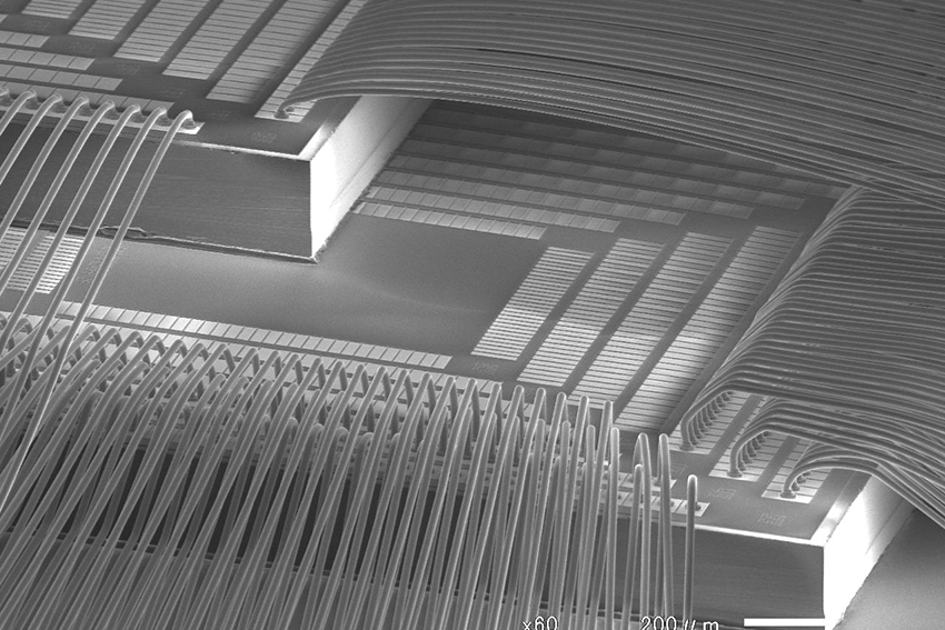
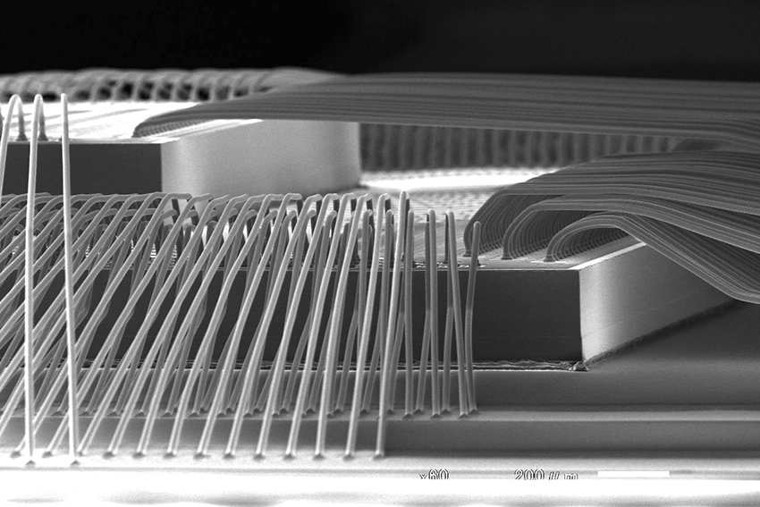
We had the possibility to take a better take a look at your EX-1P bonding wire, which encompasses a copper core with a gold-palladium alloy coating. This product seems to strike a classy stability between electrical conductivity, corrosion resistance, and mechanical reliability. May you share extra about how the EX-1 sequence was developed, and what particular improvements you launched to boost its efficiency?
The EX sequence was initially developed as a cost-effective, high-performance various to conventional gold bonding wire, which had change into more and more costly and fewer sustainable for mass manufacturing.
Within the case of EX1P, the core of the wire is made from high-purity copper, which gives wonderful conductivity. To this, we utilized a really skinny coating of gold —just a few nanometer thick— on prime of palladium coating that’s lower than 0.1 micrometer thick. Reaching this ultra-thin and uniform coating, whereas sustaining mechanical integrity and efficiency consistency, was extraordinarily difficult.
We needed to make main developments in floor therapy know-how and optimize each step of the coating and wire-drawing course of. It required us to reengineer our plating programs to function on the nano stage, guaranteeing uniform adhesion, sturdiness, and efficiency with out rising price. The result’s a product that achieves the desired trifecta {of electrical}, bonding, and environmental resilience, and it has been very properly acquired out there.
As semiconductors are more and more utilized in extra demanding environments—particularly in automotive electronics and industrial energy programs—there’s a larger want for bonding wires that may ship each excessive corrosion resistance and low electrical resistivity. This stability will be extraordinarily troublesome to attain. However your EX-1S wire seems to supply each. How does your coating know-how make this attainable?
You’re proper—the trade-off between corrosion resistance and electrical conductivity is a elementary problem in bonding wire design.
Historically, producers have sought to enhance corrosion resistance by including alloying parts to copper, creating extra sturdy supplies. Nevertheless, this method inevitably will increase electrical resistivity, which might restrict system efficiency.
Our method is totally different. We protect the high-purity copper core, which provides us the very best electrical conductivity. Then, we apply a protecting alloy coating solely to the floor—not all through the wire—so we will improve corrosion resistance with out compromising conductivity.
What makes this answer technically difficult is the precision of the coating course of. After coating, we carry out a extremely demanding wire drawing operation, which should keep uniformity and construction even at microscopic thicknesses. Our proprietary know-how permits us to management plating on the nano stage, which is uncommon on this trade.
Because of this, EX1S achieves {an electrical} conductivity of two.4 µΩcm, which is equal to traditional gold wire, whereas providing superior corrosion safety, and all at a considerably decrease price of supplies and processing. It is an instance of innovation by means of precision.
Your organization clearly locations a powerful emphasis on analysis and improvement. With over 300 patents throughout 10 international locations, that dedication is clear. May you share extra about your present R&D priorities? Are there any new applied sciences or merchandise that you simply’re at present creating?
Completely. We’re at present centered on two main areas of improvement:
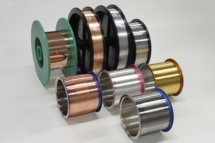
- Silver Alloy Wire – In particular functions—significantly in reminiscence gadgets—copper wire shouldn’t be all the time an acceptable choice, as a result of challenges with bonding on chips with fragile construction. Historically, gold has been used right here, however its price is a priority. To deal with this, we have now developed a silver-based alloy bonding wire. It gives decrease resistivity than gold, excessive corrosion resistance, and wonderful bondability. This product is already being utilized in some industrial functions.
- Energy Semiconductor Bonding Wire – The expansion of energy electronics, particularly in electrical automobiles and industrial programs, has created a requirement for thicker (heavy) bonding wires—sometimes round 300 microns and extra in diameter, in comparison with 18 microns in commonplace skinny wire. These thick wires should carry excessive present and stand up to thermal biking underneath excessive temperature operation.
To fulfill this want, we developed:
- LX1, a high-reliability aluminum wire designed particularly for energy semiconductor. It has strong reliability underneath high-temperature, high-current environments and meed the demanding necessities for subsequent era energy gadgets.
- BX1V, a gentle copper wire that improves bonding processability and productiveness on the manufacturing ground.
Each of those merchandise are already being utilized in real-world functions, and we’re persevering with to refine them in collaboration with clients.
We perceive that you simply’ve been very energetic on the worldwide stage, together with your common participation at PCIM Europe. These occasions are necessary for presenting know-how and constructing partnerships. How do such outreach efforts match into your worldwide technique? And are there different occasions the place you’ll be showcasing your merchandise?
Sure, we’ve exhibited at PCIM Europe for 3 consecutive years, and it has change into one in all our most necessary international platforms. PCIM is the world’s main exhibition for energy semiconductors, and it attracts a extremely certified viewers that features not solely industrial clients but additionally researchers, teachers, and system designers.
This yr at PCIM 2025, we launched the LX1 aluminum wire, and the response exceeded our expectations. We acquired quite a few inquiries from worldwide customers and new potential clients, confirming the robust market curiosity.
Along with PCIM, we might be collaborating in:
- EMPC (European Microelectronics and Packaging Convention) in Grenoble, France this fall, the place we’ll be presenting new reliability information for LX-1.
- EPTC (Electronics Packaging Expertise Convention) in Singapore in December, the place we’ll current findings associated to efficiency testing and qualification methodology.
These outreach efforts are strategic. They assist us:
- Construct belief with international stakeholders
- Current our technical management
- Kind new enterprise partnerships
- Maintain tempo with the evolving wants of worldwide markets
Will you be releasing any technical reliability information at these occasions?
Sure. At EMPC, we’ll share the outcomes of a joint analysis venture performed with a German analysis institute, Fraunhofer. We evaluated the reliability of LX1 utilizing silicon carbide (SiC) chips, and the outcomes confirmed that LX1 is 4 occasions extra dependable than typical aluminum bonding wire underneath high-temperature working circumstances.
Because the trade strikes towards SiC and GaN energy semiconductors, which might function at considerably larger temperatures than silicon, wire reliability turns into much more crucial. That is particularly related for electrical automobiles, the place thermal administration is a key concern. LX1 was designed to satisfy this problem.
At EPTC in Singapore, we are going to current a strategy to streamline reliability testing. Historically, AEC-Q006 testing requires 2,000 to 4,000 hours of analysis, which may be very time-consuming. We’ve investigated the feasibility of an accelerated testing method that entails rising the check temperature to cut back the time wanted for analysis—whereas sustaining statistical accuracy. We have documented this system in an tutorial paper, which we’ll share on the convention.
You talked about your collaboration with a German analysis institute. Are you searching for to kind extra worldwide partnerships—in R&D, in gross sales, or in product improvement?
Sure, we’re completely open to new collaborations. It is dependent upon the circumstances, in fact, however we’ve already engaged in shut partnerships with clients to develop options tailor-made to their particular semiconductor packaging processes.
As we transfer into new know-how domains—significantly in AI, energy semiconductors, and reminiscence—we’re actively contemplating new joint improvement and analysis, together with worldwide partnerships. We method these alternatives on a case-by-case foundation, with an eye fixed towards shared technical objectives and long-term worth creation.
You talked about earlier that your manufacturing websites are situated in Japan, China, and the Philippines. Are there different areas you’re concentrating on for future gross sales development or new manufacturing funding?
At the moment, we function three manufacturing amenities:
- Japan (our main R&D and know-how hub)
- China (the place we plan to relocate to a brand new, fashionable manufacturing unit to broaden capability)
- The Philippines (a key website for high-volume manufacturing)
This yr, our focus has been on scaling the Chinese language operation, which we are going to full quickly. Subsequent, we might be increasing manufacturing capability in Japan and the Philippines.
That stated, we’re continually evaluating international demand developments. Our strategic precept is to manufacture close to the client, which allows quicker supply, higher service, and improved provide chain resilience.
Your organization was based in 1975, so that you’re celebrating your fiftieth anniversary this yr, if I’m not mistaken. If we have been to return again and do that interview once more in 5 years, in 2030, is there a selected objective that you simply’ve set—one thing you want to to have the ability to say you’ve achieved by that point?
Sure, completely. Waiting for 2030, our objective is to firmly set up ourselves because the world’s primary bonding wire firm—not simply in market share, however in know-how management, product high quality, buyer belief, and international responsiveness.
To attain this, we aren’t solely specializing in strengthening our tangible property—our manufacturing {hardware}, tools, and manufacturing amenities—but additionally our intangible capabilities. That features software program programs, automation infrastructure, and the flexibility to digitally help clients anyplace on the planet.
We intention to create a world group that’s able to responding to all forms of buyer requests—whether or not they relate to superior technical specs, fast product improvement, tailor-made options, or in-depth supplies consulting. Our ambition is to change into a full-solution supplier throughout all key software areas: from automotive and AI to reminiscence, cell, and energy semiconductors.
To do that, we’re enhancing our inside programs on each stage: from product improvement to service supply, from coaching engineers to constructing seamless provide chains. We’re additionally investing closely in info programs in order that we will present not simply merchandise, however value-added help—resembling technical documentation, efficiency simulations, and design steerage—to our clients worldwide.
By 2030, we need to be the form of firm that our clients flip to first—not only for high-performance bonding wire, however for partnership, problem-solving, and innovation. That’s our imaginative and prescient for the subsequent 5 years.
Leave a Reply