Allow us to emphasize at the start the financial case for chiplet structure within the automotive programs.
The automotive business faces an unprecedented problem: integrating more and more refined digital programs whereas sustaining value competitiveness in mass manufacturing. Conventional monolithic System-on-Chip (SoC) designs, whereas functionally strong, current important financial boundaries when scaled to automotive volumes. Chiplet know-how emerges as a compelling answer, providing substantial value benefits by modularity, yield optimization, and design reuse of IP blocks.
Think about a typical superior driver help system (ADAS) controller that requires high-performance computing cores, specialised AI accelerators, a number of communication interfaces, and energy administration circuits. In a monolithic strategy, this whole system could be fabricated as a single massive chip on an costly superior course of node (corresponding to 7nm or 5nm). If any portion of this massive die has manufacturing defects, all the chip turns into unusable, leading to poor yield.
The chiplet strategy essentially adjustments this financial equation. As a substitute of 1 massive chip, the identical ADAS controller may be applied utilizing a number of smaller chips: a CPU chiplet on 7nm for efficiency, reminiscence interface chiplets on 22nm for value effectivity, analog RF chiplets on specialised processes, and energy administration on mature 65nm nodes. Every chiplet may be manufactured independently, examined individually, and solely the known-good dies are assembled into the ultimate bundle. This strategy usually reduces general system prices by 20-40% whereas bettering manufacturing yields from 60-70% to over 90%.
Understanding Chiplet Expertise – What’s a Chiplet by the best way?
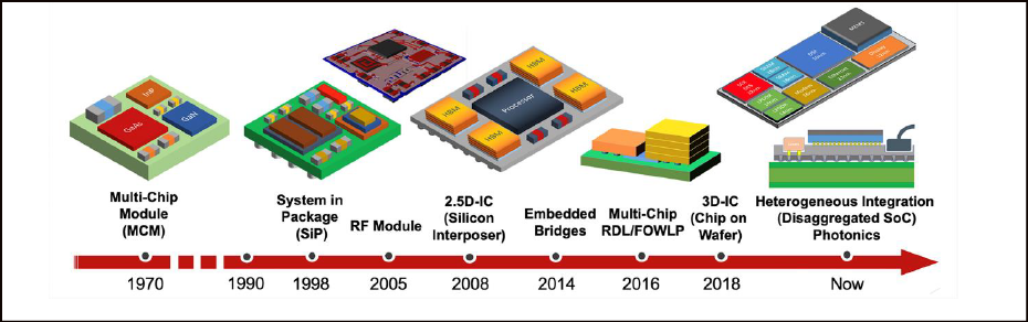
The know-how of chiplet is much from being new; the truth is, Gordon Moore in his paper “Cramming extra parts onto built-in circuits” already talked about the motion in the direction of multi-die units.

A chiplet represents a paradigm shift from conventional semiconductor design philosophy. Moderately than integrating all system features onto a single piece of silicon, chiplet structure divides advanced programs into smaller, functionally discrete semiconductor dies that talk by standardized high-speed interconnects.
Every chiplet serves a particular function inside the bigger system. Consider it as constructing with LEGO blocks reasonably than carving from a single piece of marble. For instance, a graphics chiplet handles visible processing, a CPU chiplet manages basic computation, reminiscence chiplets present storage, and I/O chiplets handle exterior communications. These particular person parts are manufactured individually, usually utilizing completely different course of applied sciences optimized for his or her particular features, then assembled in a single bundle utilizing superior packaging strategies.
The important thing differentiator lies within the interconnect requirements. In contrast to conventional multi-chip modules, the place completely different chips talk by comparatively sluggish package-level connections, chiplets use ultra-high bandwidth, low-latency interconnects corresponding to Intel’s Superior Interface Bus (AIB), AMD’s Infinity Material, or rising requirements like Common Chiplet Interconnect Specific (UCIe). These connections strategy the efficiency of on-chip communication, making the chiplet system behave functionally like a monolithic SoC, and that’s truly the place the magic occurs.
Chiplet Design

Designing chiplets requires a elementary rethinking of conventional IC design methodologies. The method begins with system-level partitioning, the place engineers, not at all times from the identical firm, should fastidiously analyze the general system necessities and establish logical boundaries for separation into particular person chiplets.
The partitioning resolution includes a number of essential concerns. Features that require frequent, high-bandwidth communication ought to typically stay on the identical chiplet to reduce inter-chiplet site visitors. Energy domains present pure boundaries, as do completely different course of know-how necessities. As an illustration, analog circuits usually require completely different course of nodes than digital logic, making them best candidates for separate chiplets.
As soon as partitioned, every chiplet have to be designed with standardized interfaces. This represents a major departure from conventional IC design, the place inner interfaces could possibly be optimized for particular implementations. Chiplet interfaces should adhere to business requirements or proprietary protocols that outline electrical traits, timing necessities, and communication protocols.
Bodily design concerns change into extra advanced with chiplets. Conventional ground planning should now account for the position of high-speed serializer/deserializer (SerDes) circuits, energy supply networks that span a number of cube, and thermal administration throughout the multi-die bundle. Sign integrity evaluation should take into account not simply on-die routing but additionally package-level interconnects and potential crosstalk between adjoining chiplets.
Verification and testing methods additionally require modification. Every chiplet have to be completely examined in isolation earlier than meeting, requiring complete built-in self-test (BIST) capabilities. Publish-assembly testing turns into tougher, as conventional boundary scan strategies could not present sufficient protection of inter-chiplet connections.

The Challenges of Integrating Totally different Chiplets on a Single Package deal
Integration challenges in chiplet programs span a number of engineering domains, every presenting distinctive technical hurdles that have to be overcome for profitable implementation.
Thermal administration represents maybe essentially the most important problem. A number of energetic cube in proximity generate substantial warmth, creating scorching spots that may degrade efficiency or trigger reliability points. Superior thermal options, together with embedded cooling constructions, thermal interface supplies, and cautious energy supply design, change into important. The thermal coefficient of growth mismatch between completely different chiplet supplies can induce mechanical stress, probably resulting in solder joint failures or die cracking over temperature cycles.
Energy supply complexity will increase exponentially with chiplet rely. Every chiplet could require a number of voltage domains with particular present and noise necessities. The bundle should present clear, steady energy to all chiplets whereas minimizing voltage drops throughout the interconnect community. Superior packaging strategies corresponding to through-silicon vias (TSVs) and embedded voltage regulators assist handle these challenges however add value and design complexity.
Sign integrity throughout inter-chiplet connections calls for cautious consideration to impedance matching, crosstalk minimization, and timing closure. Excessive-speed indicators traversing package-level interconnects face completely different challenges than on-die routing, together with better parasitics, potential electromagnetic interference, and course of variations throughout the bundle substrate.
Manufacturing and meeting current further hurdles. Recognized-good-die testing turns into essential, as changing a single faulty chiplet after meeting is usually not economically viable. Meeting processes should obtain exact alignment and bonding between a number of cube, usually with completely different sizes and thicknesses. High quality management and reliability testing change into extra advanced, as failure modes can happen on the die degree, interconnect degree, or system degree.
Software program and firmware integration provides one other layer of complexity. Working programs and drivers should pay attention to the chiplet structure to optimize efficiency, handle energy consumption, and deal with potential failure modes. Cache coherency protocols should span a number of cube, requiring cautious coordination to keep up system-level efficiency.
Instance Functions of Chiplet within the Automotive Business
The automotive sector presents quite a few compelling use instances for chiplet know-how, every leveraging the distinctive benefits of modular semiconductor structure.
Superior Driver Help Programs (ADAS) symbolize essentially the most outstanding utility space. Fashionable ADAS controllers require numerous computational capabilities: pc imaginative and prescient processors for digicam knowledge, radar sign processors, LiDAR processing items, sensor fusion engines, and safety-critical management logic. A chiplet-based ADAS controller would possibly combine a high-performance CPU chiplet for basic processing, specialised AI accelerator chiplets for machine studying inference, devoted sign processing chiplets for sensor knowledge, and safety-critical microcontroller chiplets licensed to automotive useful security requirements (ISO 26262).
This strategy gives a number of benefits over monolithic implementations. Totally different chiplets may be manufactured utilizing optimum course of applied sciences – AI accelerators on modern nodes for optimum efficiency, security microcontrollers on mature, extremely dependable processes, and analog sensor interfaces on specialised mixed-signal processes. The modular structure additionally allows scalable product households, the place primary ADAS programs use fewer chiplets whereas premium programs incorporate further processing capabilities.
Infotainment programs profit considerably from chiplet modularity. A typical automotive infotainment system requires graphics processing for a number of shows, audio digital sign processing, connectivity modules (Wi-Fi, Bluetooth, mobile), and general-purpose computing for functions. Chiplet implementation permits producers to make use of confirmed graphics chiplets from shopper electronics, specialised automotive-qualified connectivity chiplets, and cost-optimized utility processor chiplets.
Electrical car (EV) powertrains current one other compelling utility. EV management programs require high-voltage energy administration, motor management algorithms, battery administration features, and car communication interfaces. A chiplet-based strategy allows the separation of high-voltage analog circuits from delicate digital processing, improves thermal administration by distributing heat-generating features throughout a number of cube, and permits optimization of various features utilizing acceptable course of applied sciences.
Physique management modules, which handle features like lighting, door controls, window operation, and local weather programs, can leverage chiplet structure to create scalable, cost-effective options. Base configurations would possibly use minimal chiplet units for important features, whereas luxurious automobiles incorporate further chiplets for superior options.
Conclusion
Chiplet know-how represents a transformative strategy to automotive semiconductor design, providing compelling options to the business’s twin challenges of accelerating performance and value stress. The financial benefits are clear: improved manufacturing yields, diminished improvement prices by design reuse, and optimized course of know-how choice for various features may end up in system-level value reductions of 20-40% in comparison with monolithic options.
Nonetheless, profitable chiplet implementation requires mastery of latest design methodologies, superior packaging applied sciences, and complicated integration challenges. Thermal administration, energy supply, and sign integrity throughout multi-die programs demand refined engineering options. The automotive business’s stringent reliability and security necessities add further complexity to an already difficult design drawback.
Regardless of these challenges, early adopters are demonstrating the viability of chiplet approaches in automotive functions. As business requirements mature and design methodologies evolve, chiplet know-how is positioned to change into a dominant structure for advanced automotive digital programs. The know-how gives a sensible path to continued innovation in automotive electronics whereas sustaining the price constructions mandatory for mass market adoption.
The way forward for automotive electronics lies not in ever-larger monolithic chips, however within the clever disaggregation of performance into optimized, reusable chiplet constructing blocks. For automotive engineers, understanding and embracing this architectural shift might be important for creating the subsequent technology of car digital programs that ship superior capabilities at aggressive prices.
References
1 Efficient and Environment friendly Check and Prognosis Sample Era for Many Inter-Die Interconnects in Chiplet-Based mostly Packages
2 Chiplet Interconnect Testing Utilizing JTAG/Boundary Scan (ScanWorks)
Leave a Reply